Technology & innovation
AI Power Demands: Chiplets & the Future Beyond Moore’s Law
Artificial Intelligence (AI) is driving unprecedented innovations across industries, from healthcare and finance to autonomous systems. However, as AI continues to evolve, its demand for computational power and energy is growing exponentially. This surge in energy consumption, combined with slowing advancements in traditional semiconductor technology, presents significant challenges. While hardware like GPUs (Graphics Processing Units) has temporarily mitigated some bottlenecks, the semiconductor industry must now look beyond Moore’s Law for future improvements.
AI’s Growing Energy Demand
The computational demands of AI, especially for training and inference in large models like ChatGPT, have led to a sharp rise in energy consumption. Data centers, once relatively stable in terms of power usage, are now deploying increasingly powerful AI accelerators like GPUs, which consume more electricity with each generation. Reports from Goldman Sachs and the International Energy Agency (IEA) forecast exponential growth in energy demand driven by AI.
For example, Wells Fargo estimates that AI-related power consumption will grow by 550% by 2026 and could account for up to 16% of U.S. electricity consumption by 2030. This raises concerns about the sustainability of AI’s growth, underscoring the need for innovation in energy efficiency.
The End of Moore’s Law
In 1965, Gordon Moore predicted that the number of transistors on a chip would double every two years, driving continuous improvements in computing power and energy efficiency. For decades, this trend, known as Moore’s Law, fueled rapid progress in the semiconductor industry. However, in recent years, the limits of Moore’s Law have become evident. In 2017, Nvidia’s CEO Jensen Huang famously declared, “Moore’s Law is dead.”
The problem is that further shrinking transistors is no longer as feasible due to both physical and economic constraints:
- Quantum Effects: At atomic scales, quantum tunneling causes electrons to behave unpredictably, leading to power leakage.
- Heat Dissipation: The increase in transistor density generates more heat, making it harder to manage and affecting chip performance.
- Rising Costs: Advanced manufacturing techniques, such as extreme ultraviolet (EUV) lithography, are becoming prohibitively expensive, reducing the economic benefits of shrinking transistors.
As a result, the industry is now turning to alternative methods of improving performance without relying on transistor scaling alone.
GPUs: Optimizing AI Workloads and Rising Energy Consumption
GPUs have become the cornerstone of AI computation. Originally designed for rendering graphics, GPUs excel at handling AI workloads due to their ability to perform multiple calculations simultaneously (parallelism). This makes them ideal for tasks like training large-scale models and performing real-time inference.
- Scalability: Nvidia’s DGX GH200 supercomputer can link 256 Grace Hopper Superchips, offering 144 terabytes of shared memory, critical for training large AI models like GPT-4.
- Energy Efficiency: While GPUs consume significant power, they remain more efficient than CPUs for AI tasks. For instance, a GPU like Nvidia’s H100 is designed with specialized components such as Tensor Cores, which allow it to handle parallel AI workloads more efficiently than CPUs. This architecture enables GPUs to deliver significantly better performance-per-watt, especially in tasks like AI inference and training, where they excel over CPUs in both speed and energy use.
However, as AI models grow in complexity, the power consumption of GPUs continues to rise:
- Nvidia’s A100 GPU consumes 250–400W, while its successor, the H100, uses up to 700W — a 75% increase in just two years.
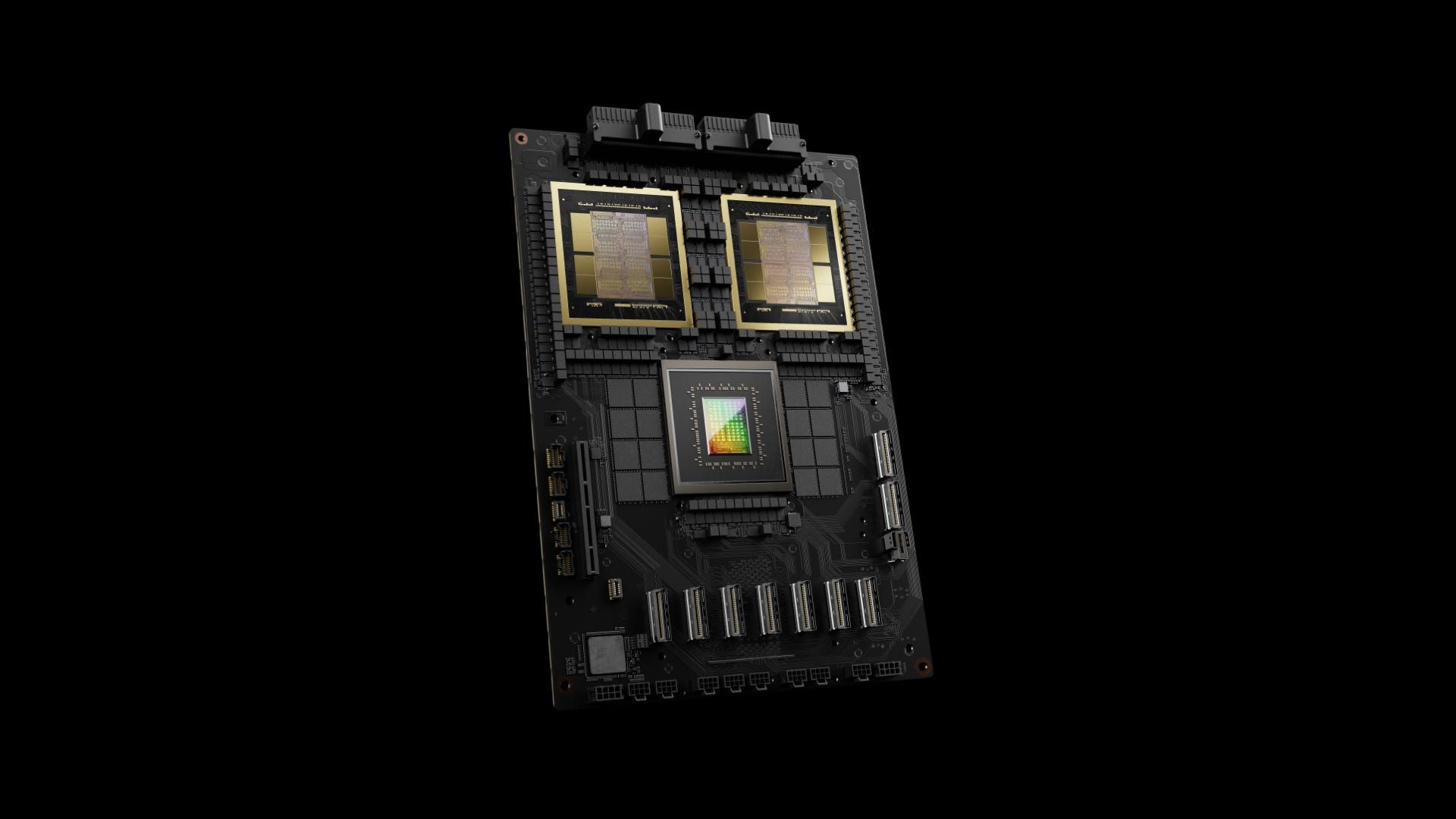
- Nvidia Blackwell B200 consumes up to 1,200W, and the GB200, combining two B200 GPUs with a Grace CPU, reaches a staggering 2,700W, representing a 300% increase over one generation.
Chiplets: Extending Moore’s Law and Unlocking New Efficiency Gains
With the limitations of Moore’s Law becoming more apparent, chiplet technology offers a viable alternative. Chiplets are small, modular components that can be integrated into a complete system, allowing manufacturers to extend the benefits of Moore’s Law by optimizing each component individually. This approach, known as heterogeneous integration (HI), enables better performance scaling, cost-efficiency, and flexibility.
The Advantages of Chiplets
- Modular Design: Chiplets allow manufacturers to combine components optimized for specific tasks. For example, high-performance CPU cores can be fabricated using advanced nodes, while less performance-critical components, such as memory controllers, can be built using older, more cost-effective technologies.
- Improved Yield: In monolithic chip designs, a single defect can ruin an entire chip. Chiplets enable defective units to be replaced individually, improving manufacturing yields and reducing waste.
- Performance Scaling: By distributing workloads more efficiently, chiplets help overcome bottlenecks like data transfer speeds between processing units, leading to better performance scaling for complex computing tasks.
Advanced Packaging Technologies
Chiplets rely on advanced packaging techniques to enable efficient communication between components:
- 3D Stacking: This allows chiplets to be stacked vertically, reducing data transfer latency and power consumption. For example, AMD’s 3D V-Cache technology demonstrated a 15% performance improvementin gaming and data center workloads.
- 2.5D Packaging: This technique places chiplets side by side on a silicon interposer, facilitating high-speed communication between components and is critical for integrating high-bandwidth memory (HBM), particularly in AI and high-performance computing (HPC) applications.
Standardizing Chiplet Communication
For chiplet-based systems to succeed, standardized communication between chiplets is essential. The Universal Chiplet Interconnect Express (UCIe) defines protocols and interfaces for chiplets, fostering interoperability. This is particularly important in AI and HPC applications, where data throughput and low latency are critical for performance.
Economic Viability of Chiplets
Chiplet-based designs offer economic advantages over traditional system-on-chip (SoC) architectures. Studies have shown that System-in-Package (SiP) architectures, which use 2.5D and 3D integration, are both technologically and economically viable. Chiplets allow manufacturers to reuse existing IP and optimize individual components, reducing production costs and extending the lifecycle of older technologies.
Real-World Applications of Chiplets: NVIDIA and AMD’s Divergent Strategies
Chiplets are increasingly becoming part of the design of high-performance computing (HPC) and AI systems. By breaking down complex chips into smaller, modular components, chiplets offer better optimization, scalability, and cost efficiency. Leading companies like Intel, AMD, and now Nvidia are leveraging chiplet architectures in different ways.
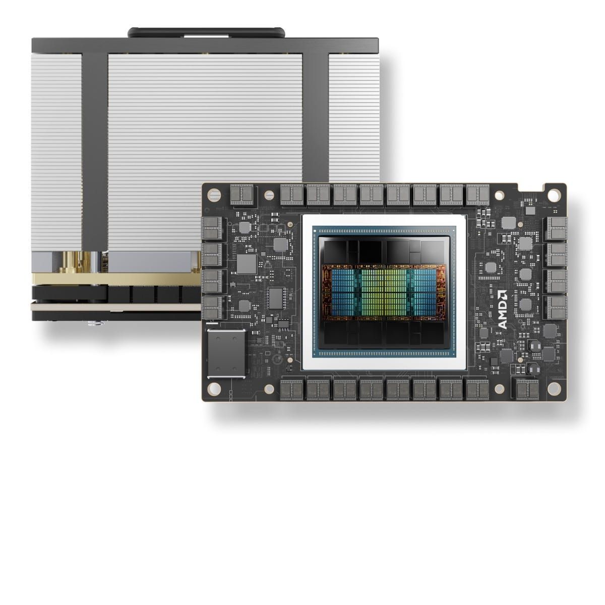
For instance, Intel’s Ponte Vecchio GPU uses 47 chiplets to pack 100 billion transistors into a single module, delivering 45 teraflops of performance. Similarly, AMD’s MI300X integrates 12 chiplets to efficiently balance compute, memory, and I/O tasks, targeting the massive computational needs of generative AI models.
However, despite both companies embracing chiplet technology, Nvidia and AMD have taken distinct approaches in implementing their strategies. These divergent paths highlight their unique ways of addressing AI workloads and computing challenges in the “More than Moore” era.
NVIDIA’s Blackwell Architecture: A Tentative Shift Toward Chiplets
NVIDIA’s Blackwell architecture (2024) represents a significant but cautious shift toward chiplet technology. Historically, NVIDIA has focused on monolithic chip designs, where all processing components are integrated into a single, large die. However, as the limits of monolithic designs become apparent, the Blackwell B200 GPU introduces a two-chiplet architecture.
- Performance Gains: By using two large chiplets, Nvidia maximizes computational power while preserving some advantages of monolithic designs. This leads to notable performance improvements, but without fully embracing modular scalability.
- Energy Efficiency: The Grace Blackwell GB200 GPU, designed for data centers, delivers 10 petaflops of performance, double that of the previous generation, but at a higher energy cost, consuming up to 2,700W.
Although this move represents a step toward adopting chiplets, Nvidia’s architecture still relies heavily on large dies, indicating that the company is cautious about fully committing to the modular scalability of AMD’s chiplet approach.
AMD’s Chiplet Strategy: A Decade of Leadership
In contrast, AMD has been a leader in chiplet adoption for over a decade. AMD’s MI300X GPU introduced in 2024, leverages a fully modular chiplet design, breaking down complex systems into smaller, specialized components, each optimized for tasks such as compute, memory, or I/O.
- Modular Scalability: The MI300X integrates 12 chiplets (four for I/O and eight for compute), allowing AMD to optimize each component individually, improving yield and reducing costs.
- Efficiency and Cost Advantages: AMD’s smaller chiplets offer better manufacturing yields compared to Nvidia’s larger monolithic chips. In the event of a defect, only the faulty chiplet needs to be replaced, reducing overall production costs.
- Advanced Packaging: AMD leads in 3D stacking technologies, where chiplets are vertically stacked to enhance communication speed and energy efficiency, critical in AI training applications.
AMD’s decade-long commitment to chiplets gives the company a distinct advantage in terms of flexibility, scalability, and cost-efficiency. This strategy positions AMD well to respond to the increasing computational demands of AI workloads.
The Competitive Landscape: AMD’s Advantage vs. NVIDIA’s Ecosystem
While AMD holds a structural advantage in terms of hardware design and cost efficiency, NVIDIA continues to dominate the AI market largely due to its comprehensive software ecosystem. NVIDIA’s CUDA platform remains the backbone for AI and machine learning development, giving it a strategic edge over AMD’s open-source ROCm alternative.
However, AMD is closing this gap, particularly following its acquisition of Pensando, which has boosted its networking and software capabilities.
- NVIDIA’s Software and Networking Edge: Nvidia’s vertically integrated approach, which combines advanced software, networking, and hardware, remains a key differentiator. The Grace Hopper and Grace Blackwell architectures integrates CPUs and GPUs, offering unmatched data movement, critical for AI workloads where data throughput is just as important as computational power.
- AMD’s Flexibility: AMD’s modular chiplet design provides greater flexibility in meeting specific customer needs. As AI models grow larger and more complex, the ability to mix and match optimized chiplets for different tasks gives AMD a competitive edge in customization, cost efficiency, and faster time-to-market solutions.
Overcoming Challenges: The Path Forward
Despite the advantages of chiplet-based architectures, several challenges remain, particularly in thermal management and latency. Stacking chiplets increases heat density, making it harder to dissipate heat effectively. However, advancements in cooling technologies and die-to-die interconnects are helping to address these issues, ensuring that performance gains don’t come at the cost of thermal inefficiency.
Chiplets also open new possibilities for heterogeneous computing, where specialized processors (CPUs, GPUs, and AI accelerators) work together within a single system to efficiently handle different tasks. For example, Nvidia’s Blackwell architecture combines CPUs, GPUs, and Data Processing Units (DPUs) to optimize performance for complex AI workloads, ensuring that data movement and processing are efficiently managed.
Conclusion
Both NVIDIA and AMD are evolving their strategies to meet the growing computational demands of AI and high-performance computing. NVIDIA’s tentative shift toward chiplets in its Blackwell architecture signals a recognition of the need for modular designs, though it remains rooted in its monolithic approach. In contrast, AMD’s decade-long leadership in chiplet design positions it strongly to capitalize on the rising demand for scalable, flexible hardware solutions.
As chiplet technology matures, the competition between these two giants will likely intensify. While NVIDIA’s robust software ecosystem and networking capabilities provide it with a significant advantage, AMD’s modular approach offers a compelling alternative that could reshape the AI hardware landscape.
Chiplets represent a viable future of scalable, high-performance computing in the More than Moore world. By enabling modular, heterogeneous integration, chiplets offer the flexibility and efficiency needed to meet the ever-growing demands of AI and HPC applications.