Technology & innovation
Inside Lightmatter’s Passage M1000 Photonic Superchip
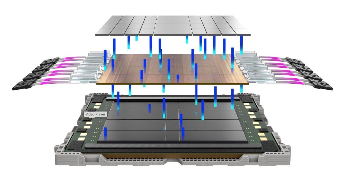
Lightmatter, a company focused on photonic supercomputing, recently announced the Passage M1000, a 3D-stacked active photonic interposer designed to deliver unprecedented bandwidth for next-generation AI and high-performance computing (HPC) workloads. Engineered for xPUs such as GPUs, AI accelerators, and switches, the M1000 overcomes the physical limitations of conventional electrical I/O by radically improving data throughput through its innovative architecture.
Key features:
- Extremely High Total Optical Bandwidth: Delivers 114 Tbps of throughput.
- 3D-Stacked Integration: Combines electrical and optical interconnects in a single package.
- Massive Die Size: Spans over 4,000 mm² using a multi-reticle approach, significantly larger than what is possible with a single reticle.
- Pervasive Optical I/O: Unlike typical edge-limited designs, optical waveguides extend across the entire chip surface, enabling “vertical” connectivity rather than being confined to the chip edges.
- 256 Optical Fiber Attachments: Each fiber can deliver hundreds of gigabits per second, with a reported 448 Gbps per fiber.
- Additional Technical Details: Incorporates 1024 Electrical SerDes operating at 56 Gbps NRZ modulation, supports 8-wavelength WDM, and is designed to handle a 1.5 kW power delivery within a 7,735 mm² package.
Why Is This Important?
Limitations of Electrical Interconnects:
Traditional electrical interposers, which serve as the foundation for connecting multiple chips in advanced packages, face a fundamental limitation known as the “shoreline” constraint. This refers to the fact that the electrical signal pins, which are the conduits for data transfer, are typically placed around the periphery or edges of each chip. This placement strategy inherently limits the number of high-speed input/output connections that can be accommodated, thus capping the effective bandwidth achievable between the interconnected chips.
As AI and HPC workloads grow exponentially, the sheer volume of data that needs to be moved between compute increasingly overwhelms these traditional methods. At ultra-high data rates, even short electrical paths suffer from significant power loss and signal degradation, further impeding performance and driving up energy consumption.
How the Passage M1000 alleviates these issues:
- Distributing Optical Waveguides: The M1000’s design embeds optical waveguides throughout its entire surface, allowing data to flow between any two points without relying solely on the chip edges. This pervasive interposer connectivity can potentially offer an exponential increase in both performance and connection density over conventional electrical systems.
- Enabling Stacked Compute Tiles: With its 3D integration, GPUs and specialized accelerators can be directly “docked” on top of the photonic interposer. This vertical stacking reduces the distance data must travel, minimizing latency, lowering power dissipation, and reducing signal degradation. A significant improvement, compared to the longer, congested pathways of traditional electrical interconnects.
This approach directly tackles the critical bottlenecks of today’s compute systems. This means a leap forward in performance and efficiency for next-generation AI and HPC workloads.
How It Stands Against Other Solutions
Existing Electrical-Based Interconnects: High-performance AI and HPC systems currently rely on established electrical solutions. For instance, NVIDIA’s latest NVLink 5.0 systems can deliver up to 1.8 TB/s bidirectional bandwidth per GPU, aggregating to significant intra-node bandwidth in configurations with multiple GPUs. InfiniBand NDR offers up to 400 Gbps per port (or 800Gbps), scaling up to around 51.2 Tbps per switch, while emerging Ethernet standards are on track to achieve terabit speeds. Despite these advancements, Lightmatter’s M1000, with 114 Tbps total optical bandwidth, represents a substantial leap in performance.
Co-Packaged Optics (CPO) vs 3D Photonics: Co-Packaged Optics integrates optical transceivers next to switch ASICs to reduce electrical trace lengths, enhance signal integrity, and lower power consumption. However, CPO still relies on routing signals primarily from the chip’s edge. In contrast, the M1000 utilizes a 3D photonic interposer that disperses optical waveguides across the entire chip surface beneath stacked compute tiles. This “edgeless I/O” design significantly enhances bandwidth and flexibility. It also positions it as a more revolutionary solution compared to CPO alternatives like Lightmatter’s own Passage L200 series.
Hyperscalers’ In-House Silicon: Major cloud providers such as AWS, Google, and Microsoft are advancing their custom silicon solutions. For instance, AWS Trainium, Google TPU, and Microsoft Azure Maia to optimize AI acceleration. These hyperscalers currently rely on external networking, whether optical or high-speed electrical, to connect their data center clusters. The M1000’s superior interconnect bandwidth and efficiency make it a compelling option for integration into these large scale infrastructures. Alternatively, given their expertise, these companies might develop proprietary photonic packaging to meet future demands.
The launch of the M1000 in summer 2025 will serve as a pivotal moment, potentially setting new benchmarks in interconnectivity for AI and HPC applications.
Manufacturing Complexity, Production Readiness and Ecosystem Maturity
The advanced 3D-stacked architecture of the M1000 presents significant manufacturing challenges. Integrating optical and electrical components across a massive, multi-reticle die while ensuring precision alignment and reliable performance at scale is no small feat. However, it appears that Lightmatter is addressing these challenges through strategic partnerships with leading industry players in fabrication, packaging, and assembly.
GlobalFoundries’ Fotonix Platform: Lightmatter is leveraging GlobalFoundries’ Fotonix platform to manufacture the M1000. Fotonix is a monolithic silicon photonics solution that integrates lasers, modulators, photodetectors, and CMOS logic on a single wafer. It eliminates the need for discrete optical components. This platform forms the foundational layer of the M1000, enabling tightly integrated, high-performance optical signaling directly within the chip’s silicon substrate.
Amkor Advanced Packaging: To address the requirements of multi-die 3D stacking, Lightmatter has partnered with Amkor Technology. Their expertise in advanced packaging is critical to realizing the M1000’s vertical integration. Amkor expertise lies particularly in aligning optical waveguides, attaching dense fiber arrays, and managing power delivery in 3D assemblies. Also, their ability to execute high-yield, high-precision packaging processes at scale will be a key determinant of the platform’s commercial viability.
ASE Partnership: Lightmatter has also partnered with ASE, a leader in semiconductor assembly and test services. ASE brings specialized capabilities in photonics-optimized 3D packaging and thermal management (essential for large-format chips like the M1000 that must dissipate up to 1.5 kW of power). ASE’s role in volume manufacturing and validation could help Lightmatter bridge the gap between innovative design and production-grade reliability.
As the M1000 moves closer to its expected launch in summer 2025, the success of this collaborative ecosystem will play a critical role. Its success will determine whether the platform can scale from proof-of-concept to mainstream adoption.
Future Roadmaps for Hyperscalers and Enterprise Data Centers
As hyperscale data centers continue to demand higher bandwidth and lower latency, the M1000 could represent a shift in AI infrastructure. Its performance and production readiness may drive major cloud providers to move away from traditional electrical interconnects and adopt fully integrated photonic superchips. This shift has the potential to redefine how next-generation HPC systems are designed and deployed.
Implications
Enabling Larger AI Models and Faster Training: The M1000’s massive optical bandwidth allows data to move more freely between GPUs or xPUs in a cluster, enabling the training of significantly larger models. This opens the door to models with more parameters and longer context windows without being bottlenecked by interconnect limitations. Faster interconnect speeds also reduce training time by minimizing idle cycles and ensuring GPUs remain compute-bound rather than I/O-bound. In HPC, this can improve weak scaling performance, where system efficiency is preserved as the problem size and compute resources scale together.
Transforming Multi-GPU Inference: Larger models require multi-GPU inference setups due to their high memory demands. Current solutions often rely on complex high-speed networking, which introduces latency and complexity. The M1000’s integrated optical interconnects drastically reduce communication latency with short-hop, high-throughput optical lanes.
This makes multi-GPU inference more efficient and lowers system design complexity by reducing reliance on external networking components and cabling. Therefore, streamlining the deployment of large inference systems.
Lowering Total Cost of Ownership at Scale: Optical signaling is inherently more power-efficient than electrical signaling at high data rates and over longer distances. In hyperscale environments, even modest improvements in power efficiency can result in substantial operational savings.
Lightmatter claims that the M1000’s photonic interposer design can reduce power consumption significantly (by 10x to 100x) compared to conventional GPUs. This is achieved through minimized SerDes usage and more efficient interconnect pathways. This enhanced performance per watt could make the M1000 a cost-effective solution for large AI and HPC deployments.
Meeting Escalating Bandwidth Demands: The trajectory of AI and HPC innovation continues to demand ever-higher interconnect bandwidth. Trillion-parameter language models and exascale computing workloads require fast, reliable data movement across thousands of nodes.
Advanced memory like HBM and next-generation interconnects are critical to breaking through the memory wall. The Passage M1000, with its claimed 114 Tbps of optical bandwidth, is well-positioned to meet these requirements, making it a compelling solution for next-gen AI and HPC infrastructure.